T5E interviews recent alumni across a wide variety of industries who have spent a year or more at their respective firms. We hope this will enlighten current students with respect to what companies look for while recruiting undergraduates and help them make more informed career choices.
What does NVIDIA do?
Nvidia is a digital IC design company that makes Graphics Processing Units and processors for mobile phones and computers. All aspects of digital design are handled in this company, from design to validation and testing.
What does your work at NVIDIA involve?
I work as a part of the physical design team that is responsible for the layout of a chip once its RTL (Register Transfer Level) is frozen. At the end of the day it involves running a tool.
A physical design engineer ensures that the digital circuits work even after the transistors and wires are etched out on silicon. The folks that design the digital circuits work with ideal wires, and their designs may not be valid when the parasitic parameters (resistance and capacitance) of the wires are taken into account. So this process warrants one to check if the circuits work even after these parasitic factors are considered. That is where a physical design (PD) engineer comes in. A PD engineer uses a tool to simulate the circuits after the cells and wires are placed, and in case the circuits don’t work in simulation, he makes changes to the location of these cells on the chip so that these parasitics are minimized. Since there are a HUGE number of cells involved in a digital chip, these movements, corrections and tests are heavily automated, and there is a tool that is intelligent enough to work out a placement and wiring strategy, but it needs an individual with a higher intellect (a PD engineer!) to lay down the initial placement of a few bigger cells, on top of which it optimizes the entire chip design. Sometimes a PD engineer needs to write down a few codes too (in TCL/PERL) to help change the automation to take care of a few specific parts of the circuits or area on the chip. Once the circuit works in simulation, and the PD folks are satisfied, they send the chip to fabrication (a.k.a Tapeout).
What is the work environment like?
Probably one of the biggest plus points of working at Nvidia is the work atmosphere. The people are extremely helpful and the work ethic is good – people understand when one is busy with some other work and don’t hesitate to pitch in with help at any time. And like in most other companies these days, you get to work from home! Of course, the free lunch, free travel, free goodies once in 6 months and the occasional ice cream/chat at 4PM everyday makes the stay all the more Christmassy.
What does NVIDIA look for while recruiting undergraduates?
They only look for solid grounding in Digital Circuits and/or Verilog (coding in TCL, PERL is a huge plus) for the hardware engineer profile. Just be frank with them. The course on Digital IC design and Digital Circuits, and one lab on Verilog is more than enough to crack the interview.
What are the career prospects beyond (or in) NVIDIA?
You could work really hard in multiple domains like verification and physical design and become a top contributor for the company. Generally, folks with experience in both verification and physical design are considered to be very helpful in any digital IC company. So one could change firms and keep yanking up their pay. One could also develop a good amount of knowledge that could help one kick-start a career in computer architecture, which is at the pinnacle of the whole digital industry. Of course, the prospects of going up the managerial ladder also exist.
Any final thoughts…
Well, the industry is a really different place. One thing that definitely changes is that you don’t refer to your bosses as Sir/Ma’am. This is the first thing that I learnt from my manager, who, by the way, is from Ganga hostel!
The atmosphere is not at all academic, which is why working for a year is the best thing for the folks who are confused about higher studies. It makes one really understand whether one disliked the ‘academic life’ at IITM just because everyone else did, or if one genuinely hated it.
Also, if one wishes to settle in India, just a B.Tech from a good place like IIT is more than enough to survive in the industry. A B.Tech from IIT is considered at par with an MS/M.Tech from IISc/IIT or some university abroad, and pays too will eventually even out. An MS abroad is useful only if one wishes to settle in the US or work there for some time, because industries there prefer folks from the universities in the US itself to those from elsewhere.
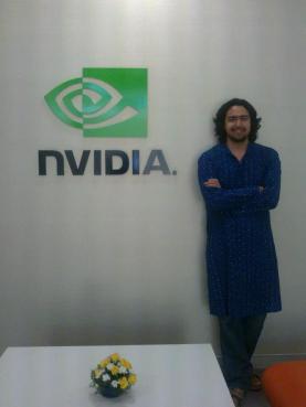
Anmol Kachroo (B.Tech/EE/2011) was a resident of Jamuna hostel. During his time at the institute, he completed a record number of courses in analog circuits and design and also did his B.Tech project under Prof. Shanthi Pavan.
If you are an alumnus and you have a story to contribute about your first job, write to us at t5e.iitm [at] gmail [dot] com and we will get in touch with you.
Editor’s note: The views expressed here are those of the interviewee alone and do not represent the views of, or should not be attributed to, NVIDIA.


